

24V Drive Screener + Guide
24V GaN Three Phase Motor Drive Board
Compare loss, ripple and cooling assumptions for a 24V DC input and U/V/W motor outputs.
Request an OEM engineering reviewFirst recorded · Evidence reviewed · By GaN Servo
1. Key Engineering Conclusions
Here, 24V is the nominal DC input, not three-phase mains. Use a 24V GaN three phase motor drive board when the motor, switching loss and packaging requirements justify it. The tool above compares scenarios; the report identifies what evidence is still needed to select or commission a custom PCBA.
| Conclusion | Evidence or basis | Decision boundary |
|---|---|---|
| Low-inductance motors can justify higher PWM. | TI TIDA-00909 | Compare motor ripple against extra bridge loss; no universal optimum frequency. |
| GaN has no PN body-diode reverse recovery. | EPC explanation of reverse conduction | Reverse channel conduction, capacitance loss and gate timing still require review. |
| In-line sensing needs a sampling budget. | TI INA240 documentation | Bandwidth and PWM rejection do not imply arbitrary ADC timing. |
| Reference designs are architecture evidence. | EPC9146 guide, revision July 2022 | Their operating conditions do not establish GanServo board ratings. |
| Thermal and production limits remain unqualified. | No board-specific measurements supplied on this page. | Request device curves, thermal tests, protection evidence and a manufacturing acceptance plan. |
2. Method, Assumptions & Unknowns
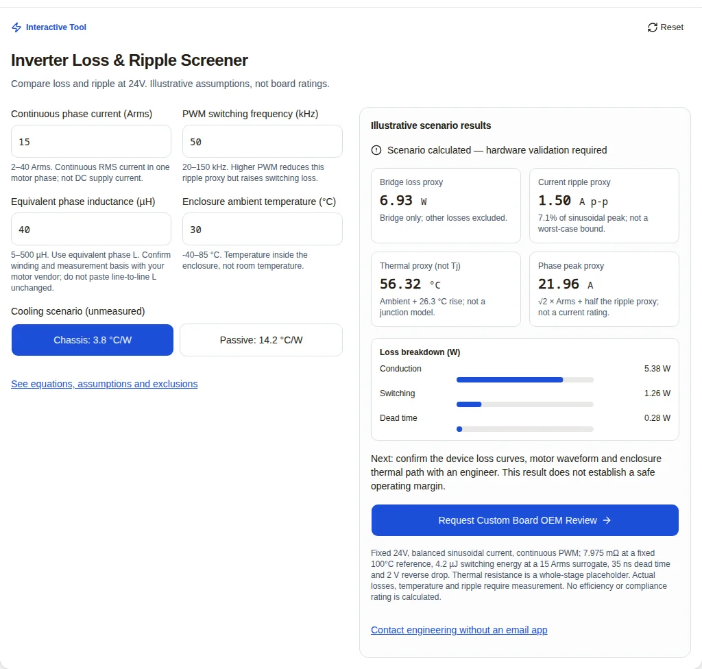
All numerical device parameters below are illustrative scenario assumptions, not claimed typical values or values extracted from the reference boards. The model assumes a fixed 24V bus, balanced sinusoidal phase current and continuous switching of all six devices. It updates synchronously in your browser.
| Output | Equation / chosen coefficient | Interpretation and exclusions |
|---|---|---|
| Conduction (W) | 3 × I² × R; R = 5.5 mΩ × [1 + 0.006 × (100 − 25)] = 7.975 mΩ | R is fixed at a 100°C reference, not solved at the output temperature. Linear temperature factor is illustrative. |
| Switching (W) | 6 × f × 4.2 µJ × (I / 15 Arms) | Eon + Eoff per device; RMS current used as a surrogate, not integrated over a sine cycle. Device curves and nonlinear capacitance are not modeled. |
| Dead-time conduction (W) | 6 × f × 35 ns × 2 V × (2√2/π) × I | Uses average absolute sinusoidal current. Actual timing and reverse voltage vary. |
| Ripple proxy (A p-p) | 24 / (8 × Lphase × f) | Fixed-coefficient trend only, not a worst-case SVPWM bound. Excludes electrical angle, saturation, back-EMF and modulation dependence. |
| Thermal proxy (°C) | Ambient + bridge loss × Rθ; Rθ = 3.8 or 14.2 °C/W | Whole-stage placeholders; not junction temperature. No thermal feedback, device gradients or measured interface resistance. |
| Phase peak proxy (A) | √2 × I + ripple proxy / 2 | No transient overload, controller fault or saturation prediction. |
| Not calculated | Gate-drive, logic, copper, shunt, capacitor and motor losses; DC-link RMS current; efficiency | Output power, modulation and actual component data are missing. These quantities must not be inferred from the displayed bridge loss. |
The 30% ripple flag is an editorial review trigger, not a motor specification. A thermal proxy above 100°C exceeds the resistance reference and may understate loss. A result below either trigger is still unqualified. To compare a real design, obtain equivalent phase inductance with its winding and measurement basis and replace the assumed device and thermal parameters in a detailed engineering assessment.
3. Three-Phase GaN Bridge Topology
Three half bridges synthesize the motor phase voltages. The DC-link commutation loop, gate return and phase-current sensing path must work together. TI TIDA-00909 documents this topology with integrated GaN half bridges and shunt-based sensing.
Follow the selected device’s layout and gate-voltage requirements. A short loop reduces parasitic effects, but neither a layer count nor a nominal loop-inductance target guarantees freedom from ringing. Check the actual assembly at supply, current and temperature extremes.
4. PWM Frequency, Ripple & Motor Heating
At fixed inductance the tool’s ripple proxy falls inversely with PWM frequency. That relationship supports comparing scenarios; it does not establish rotor eddy loss, torque accuracy, acoustic noise or a stable current-loop bandwidth. Those depend on the motor and control system.
| PWM (kHz) | Ripple proxy (A p-p) | Bridge loss proxy (W) | Next check |
|---|---|---|---|
| 20 | 3.75 | 6.00 | Measure winding current, motor heating and inverter temperature at the same operating point. |
| 50 | 1.50 | 6.93 | Measure winding current, motor heating and inverter temperature at the same operating point. |
| 100 | 0.75 | 8.47 | Measure winding current, motor heating and inverter temperature at the same operating point. |
5. Modulation & Timing Budget
The calculator does not switch between modulation methods. Continuous PWM is its comparison baseline. Discontinuous PWM can reduce commutations, but loss changes depend on electrical angle, power factor, modulation and switching energy. Do not apply a fixed percentage saving to this model.
Verify the timing budget at the shortest pulse, not only at the nominal PWM period. Dead time must prevent overlap across component and temperature variation while limiting reverse conduction. The tool’s 35 ns is an assumption and must not be copied as a firmware limit.
6. Phase Current Sensing & Control
TI INA240 documentation documents a current-sense amplifier with enhanced PWM rejection and a 400 kHz small-signal bandwidth. That bandwidth is not a promise of sub-200 ns settled samples. Consult the datasheet’s specific step and recovery conditions and budget the complete ADC signal chain.
| Architecture | Benefit | Constraint | Validation |
|---|---|---|---|
| In-line phase shunts | Phase-current visibility beyond low-side conduction windows | Common-mode transients, shunt heating, amplifier recovery | Measure settling and offset at operating PWM and phase voltage. |
| Low-side shunts | Ground-referenced measurement and potential cost savings | Sampling window varies with duty and modulation | Check reconstruction at high modulation and minimum pulse. |
| Magnetic sensing | Can provide isolation with a suitable part | Footprint, offset drift, bandwidth and cost are device-specific | Verify sensor range, delay and required isolation rating. |
7. Public Evidence & Scope Boundaries
These primary sources were reviewed on . They establish examples and component behavior; they do not validate this calculator’s coefficients or a GanServo production board.
| Source | Published scope | What it supports | What it does not prove |
|---|---|---|---|
| TI TIDA-00909 | 12–60V input, 7 Arms / 10 Apeak; tested up to 100 kHz | A low-voltage GaN three-phase inverter and current-sensing implementation. | Current capability or thermal performance of a different 24V PCBA. |
| TI TIDA-010273 | 250W appliance inverter using the 650V DRV7308 GaN IPM; 15 kHz example | A different voltage class and integration approach. | A low-voltage LMG5200 design, 24V suitability, or this tool’s loss values. |
| EPC9146 guide, revision July 2022 | 400W three-phase BLDC evaluation board using EPC2152; see guide for operating limits | An evaluation topology, protection and commissioning workflow. | Qualification of an enclosed actuator, a replacement board, or a current production availability claim. |
| TI INA240 documentation | INA240 current-sense amplifier datasheet and application material | PWM rejection and signal-chain design considerations. | A universal sampling delay, exact ADC accuracy or a complete protection rating. |
| EPC explanation of reverse conduction | EPC technical support explanation of eGaN reverse conduction | No parasitic PN body diode; reverse conduction still matters. | Zero switching loss or a universal safe dead time. |
8. GaN, Silicon & Integrated Alternatives
Compare complete implementations at the same bus voltage, motor waveform, current, PWM, ambient and cooling boundary. This page supplies no measured GaN-versus-silicon efficiency, size or price comparison.
| Option | Reason to evaluate | Cost or integration risk | Evidence needed |
|---|---|---|---|
| Discrete low-voltage GaN | Compact high-frequency switching where motor ripple matters | Driver, layout and assembly effort; unit pricing depends on BOM and volume | Matched loss curves, ringing and thermal characterization. |
| Integrated GaN half bridge | Reduced gate-loop integration work | Package thermal path, interfaces and sourcing constrain the design | Vendor reference files plus tests in the final enclosure. |
| Low-voltage silicon MOSFET | May be suitable where switching requirements are modest | Reverse recovery and gate-drive behavior are part-specific; no generic efficiency penalty assumed | Same-condition thermal and efficiency comparison. |
| Existing qualified motor drive | May reduce firmware and qualification effort | Envelope, interfaces, supplier lifecycle and purchase cost | Confirm ratings and application compatibility against a current supplier specification. |
9. Thermal, Regeneration & Misuse Boundaries
A 24V nominal label does not define maximum bus voltage. Battery charge level, returned mechanical energy and switch-node overshoot must fit every component’s limits. Device voltage headroom is not an energy absorber.
| Risk | Failure or cost mechanism | Mitigation / alternative |
|---|---|---|
| Model misuse | A proxy is treated as a safe current or junction rating | Use selected-part curves and a coupled thermal model; qualify the final assembly. |
| Thermal bottleneck | Unequal switch loss, solder or interface resistance creates a hot spot | Measure device and board temperatures at sustained load and maximum enclosure ambient. |
| Regenerative overvoltage | Non-receptive supply cannot absorb returned energy | Size a receptive supply or brake path for energy and repetition; do not rely on a TVS for sustained braking. |
| Scenario mismatch | Saturated inductance, unbalanced phases or DPWM invalidate assumptions | Use the actual waveform and motor model; measure worst operating points. |
| Cost and supply | A compact device increases assembly, test or sourcing cost | Compare total BOM, fixture, yield and lifecycle costs; consider silicon or a qualified module. |
| Fault response | Blanking and comparator-to-gate delay allow excessive fault energy | Establish part-specific fault limits and validate using a controlled protection fixture. |
10. EMI & Installation Evidence
No emissions spectrum or compliance result is available for the proposed custom PCBA. CISPR 25 and IEC 61800-3 requirements depend on the product and installation; the tool does not choose a standard, class or filter. Confirm the applicable edition, category, test method and acceptance limits with the qualification team.
Control the commutation loop and local decoupling first, then assess common-mode and differential-mode paths. Select filters from measured noise and source impedance, checking resonance and supply stability. Cable length, chassis coupling, leakage constraints and the motor winding affect the result. A generic choke, capacitor value or spread-spectrum setting is not a compliance recipe.
11. Worked Scenarios — Calculated, Not Field Tests
These hypothetical examples use exactly the published tool model. They are not customer projects or measured production outcomes. Unless stated otherwise: 24V, 15 Arms, 50 kHz, 40 µH equivalent phase inductance and 30°C ambient.
| Scenario / change | Calculated proxies | Interpretation | Next action |
|---|---|---|---|
| A: PWM tradeoff | 8.47 W; 0.75 A p-p; 62.2°C thermal proxy | 100 kHz halves the default ripple proxy, while switching loss increases. | Compare measured motor and bridge heating before selecting PWM. |
| B: Passive enclosure | 6.93 W; 1.50 A p-p; 128.4°C thermal proxy | Passive 14.2°C/W raises the thermal proxy above the 100°C reference; fixed-R loss may be understated. | Improve heat extraction or reduce current; request thermal review. |
| C: Low-inductance motor | 1.48 W; 5.00 A p-p; 35.6°C thermal proxy | 6 Arms and 12 µH give a larger ripple-to-peak ratio despite lower conduction loss. | Confirm inductance under load and check winding current with a suitable probe. |
12. OEM Manufacturing & Acceptance Plan
This is a proposed review checklist, not a claim of certified factory processes or verified production tolerances. Package-specific assembly guidance and the agreed reliability requirements govern the inspection and test plan.
| Review item | Required artifact | Acceptance decision |
|---|---|---|
| Layout and stackup | Device layout comparison, fabrication stackup, copper and thermal-path review | Resolve commutation-loop, gate-return and heat-flow issues. |
| Assembly process | Stencil/reflow recommendations, handling rules for selected part MSL, supplier process record | Agree the process for the actual package; no universal MSL assumption. |
| Solder and inspection | AOI/AXI coverage, package-specific void criteria and representative images | Agree acceptance criteria rather than claiming a universal IPC void percentage. |
| Electrical test | Fixture coverage, rail checks, sensor calibration and traceability records | Define limits for each board and an escalation path for failures. |
| Protection and thermal test | Fault timing and energy record, sustained-load data and temperature map | Confirm the complete assembly meets the application limits. |
| Quality and lifecycle | Current facility certificate and scope if required, change-control plan and approved BOM | Verify applicability and sourcing before committing volume. |
Prepare an RFQ with continuous phase Arms, instantaneous peak A and duration, supply min/max and returned braking energy, motor data and inductance basis, mechanical envelope, enclosure ambient, cooling interface, sensor/firmware interfaces, target volume and required qualification. Review our quality evidence and turnkey manufacturing guide, then request project-specific documentation.
13. Frequently Asked Questions
Estimator & Calculation
What does this calculator actually predict?
It compares illustrative six-switch bridge loss, a fixed-coefficient ripple proxy and a lumped thermal proxy at 24V. It does not predict efficiency, motor temperature, safe continuous current or production board ratings. All coefficients and exclusions are listed in the method section.
Which inductance should I enter?
Enter equivalent per-phase inductance for the operating point. Line-to-line measurements need conversion appropriate to the winding connection and measurement method. Obtain the basis, test frequency, rotor position and saturation information from the motor vendor; an unknown inductance needs engineering review.
Why does higher PWM reduce the ripple number?
The screening proxy is 24/(8Lf). Holding phase inductance fixed, doubling PWM halves that proxy. The coefficient is a simplification; actual SVPWM ripple varies with duty, electrical angle, back-EMF, winding and modulation. The proxy is not a worst-case bound or a prediction of rotor heating.
Are these device parameters measured GanServo specifications?
No. On-resistance, its temperature multiplier, switching energy, dead time, reverse voltage and thermal resistance are explicitly chosen scenario assumptions. They are not fitted to the cited reference designs. Replace them in an engineering model with the selected part data and measurements before selecting a board.
Why are no results shown for blank or out-of-range inputs?
A missing or unsupported input cannot produce a useful comparison. Correct the marked field or reset to the default example. If motor data is unavailable, contact engineering with the motor datasheet instead of substituting zero.
Electrical & Inverter Architecture
Is phase Arms the same as DC supply current?
No. Phase Arms describes heating in a motor winding. DC current depends on real output power, bus voltage and losses. Specify continuous phase Arms and peak instantaneous amperes with duration separately, plus the supply current limit.
Does GaN remove every switching loss?
No. Enhancement-mode GaN avoids the parasitic PN body diode reverse recovery found in silicon MOSFETs. Output capacitance, gate charging, voltage-current overlap and reverse channel conduction still matter. Zero reverse recovery does not prevent shoot-through or ringing; see the EPC device explanation in References.
Can I use the tool’s 35 ns dead time in firmware?
No. It is an illustrative model input. Minimum dead time depends on driver delay mismatch, gate network, PCB parasitics, device characteristics and temperature. Verify overlap and reverse conduction on the actual assembly before setting firmware limits.
Can in-line sensing sample at any time?
In-line sensing avoids some low-side shunt measurement windows, but common-mode transients, amplifier settling, output swing, ADC acquisition and blanking still constrain sampling. PWM rejection is not a guarantee of instantaneous settling.
Can a higher device voltage rating absorb regenerative braking?
Voltage headroom alone does not absorb energy. Measure maximum bus voltage and switch-node overshoot and provide an energy path into a receptive battery, regenerative supply or appropriately rated brake circuit. Size that path for the mission profile.
Thermal & High-Frequency EMI
Is the thermal result a junction temperature?
No. It is ambient plus modeled bridge loss times an assumed whole-stage thermal resistance. It omits device-to-board gradients, nonuniform losses and temperature feedback. A proxy above the fixed 100°C resistance reference flags an inconsistent scenario; values below it still require hardware qualification.
Does a higher PWM frequency guarantee a silent, cooler motor?
No. Reduced current ripple can help some low-inductance motors, but switching loss rises in this model. Acoustic noise and rotor losses depend on harmonics, motor geometry, speed and mechanical resonances. Measure the complete motor-drive system.
Which EMI filter guarantees compliance?
No universal filter guarantees compliance. Choose the applicable product standard and installation class, then evaluate input impedance, cable routing, chassis coupling and emissions using the specified setup. Tune the filter from measurements and confirm stability, leakage and thermal limits.
Can a TVS handle sustained braking energy?
Do not assume it can. A TVS pulse rating is not a continuous energy rating. Compare kinetic energy and repetition rate with the battery or brake resistor absorption capability, and check component temperature and bus overvoltage during a fault.
How should I select DC-link capacitors?
Use simulated or measured capacitor RMS current over modulation and power factor, plus ESR heating, voltage derating, DC bias and layout inductance. Place suitable high-frequency decoupling close to the commutation loop and provide bulk energy storage separately. This tool does not calculate a capacitor current rating.
OEM DFM & Testing
What should an OEM review request include?
Send supply limits, regenerative energy, continuous and peak phase current with duration, the motor datasheet and inductance basis, envelope, enclosure ambient, cooling interface, firmware and sensor interfaces, required qualification, and expected volume.
Is a particular layer count mandatory?
No universal layer count establishes reliability. Follow the selected device reference layout and review current loops, gate return, creepage or clearance requirements, copper temperature rise, thermal vias and assembly constraints for the actual stackup.
Is a fixed solder void percentage an IPC guarantee?
No universal void percentage is claimed here. Agree acceptance criteria using package vendor guidance, the selected assembly standard, thermal performance and application reliability requirements. Record inspection coverage and traceability in the manufacturing plan.
Is short-circuit protection proven by the estimator?
No. Establish the selected device’s fault limits and test the complete comparator-to-gate path, including sensing delay, blanking and fault energy, using a controlled fixture. Neither the model nor these public references certify GanServo protection timing.
Does this page certify factory capability or a medical or automotive design?
No certification or customer qualification is asserted. The scenarios are hypothetical and production evidence is not supplied here. Request the relevant facility certificate, scope, current process records and application-specific validation plan during supplier review.
14. References & Evidence Status
Reviewed . Linked primary sources are the basis for the scoped manufacturer statements above. Public production measurements, customer case records, compliance reports and facility certification evidence are not supplied here; request them for the actual program. The numerical model remains an illustrative comparison, not an independently validated board model.
- TI TIDA-00909 — low-voltage inverter reference; design guide revision April 2017.
- TI TIDA-010273 — appliance inverter using DRV7308; design guide June 2024. Different voltage class.
- EPC9146 guide, revision July 2022 — 400W inverter architecture and commissioning documentation. No current availability claim.
- TI INA240 documentation — device characteristics, PWM rejection and settling conditions.
- EPC explanation of reverse conduction — device reverse-conduction behavior; published February 2022.
Explore Adjacent 24V GaN Servo Hardware
Compare companion controller PCBAs, servo amplifiers, and integrated stacks for low-voltage actuation:
Inquiry Email
Include target torque/speed, quantity, and delivery location.