

24V Module Screener + Guide
24V Low Voltage GaN Servo Module
Screen power stage loss, high-frequency phase current ripple, and thermal rise for compact 24V robotic joint and gimbal servo drives.
Request an OEM engineering reviewFirst recorded · Evidence reviewed · By GaN Servo
1. Engineering conclusions for a 24V low voltage GaN servo module
Use the screener to compare candidate operating points before requesting a custom module review. Public reference hardware supports exploring this architecture; it does not establish GanServo product ratings.
PWM trades ripple against bridge loss
In this model, 20 → 100 kHz divides ripple by five while increasing switching and dead-time loss fivefold. Compare the calculated table; motor losses remain unknown.
GaN is a candidate, not an automatic winner
TI TIDA-00909 demonstrates a low-voltage GaN inverter. Select silicon or GaN using loss, layout, sensing, cost, and validation effort at the same operating point.
Cooling changes the result materially
The default scenario gives a 19.88°C rise with the 4.2°C/W assumption versus 70.05°C at 14.8°C/W. These are assumed paths; see thermal limitations and EPC9146 guide, revision July 15, 2022.
Qualification data is still required
Current rating, efficiency, outline, encoder support, certification, and production process capability are not established here. The evidence checklist defines the next review.
2. Reproducible method, assumptions, and limits
All numerical tables and charts below use the same function as the tool. Values are illustrative assumptions selected for sensitivity screening, not extracted device measurements. The model assumes balanced sinusoidal phase current and does not solve thermal feedback.
| Quantity | Assumed value | Meaning / limitation |
|---|---|---|
| On-resistance reference | 5 mΩ at 25°C; 0.006/°C linear coefficient | 7.25 mΩ at a fixed 100°C reference, not a selected FET curve. |
| Switching energy | 3.8 µJ per device at 24 V / 12 Arms | Aggregate screening parameter; linear voltage/current scaling is unvalidated. |
| Dead time / reverse drop | 30 ns / 2.0 V | Loss assumptions, not recommended gate settings. |
| Effective thermal path | 4.2 or 14.8 °C/W | Comparison assumptions, not package thermal resistances or measured chassis paths. |
| Flags | 100°C thermal reference / 25% ripple-to-peak | Model boundary / editorial review trigger; neither is a safe operating limit. |
Pcond = 3 × Irms² × R100
Psw = 6 × fsw × Eref × (Irms / 12 A) × (Vbus / 24 V)
Pdead = 6 × fsw × 30 ns × 2 V × (2√2 / π) × Irms
ΔIpp = Vbus / (8 × Lphase × fsw)
Pbridge = Pcond + Psw + Pdead; ΔTproxy = Pbridge × Rθassumed
Tproxy = Tambient + ΔTproxy; Ipeak proxy = √2 × Irms + ΔIpp / 2
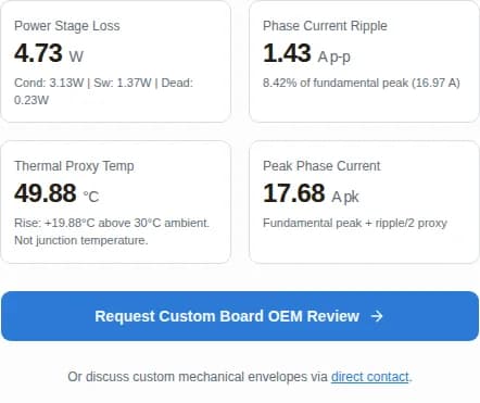
For the default 24 V / 12 Arms / 60 kHz / 35 µH / 30°C case: bridge loss 4.73 W, ripple 1.43 A p-p, thermal proxy 49.88°C with direct cooling. Excluded: gate/logic rails, shunt and copper loss, motor core and winding loss, regeneration, modulation angle, switching transients, and control-loop dynamics. The ripple expression is not a worst-case SVPWM bound.
3. Define the module boundary before choosing parts
Specify whether “module” means a power-stage daughterboard, an integrated FOC board, or an enclosed drive. Allocate power input protection, local decoupling, energy absorption, sensing, auxiliary rails, encoder interfaces, fault shutdown, and heat removal explicitly. The drawing is an architectural checklist, not a GanServo pinout.
The public EPC9146 guide, revision July 15, 2022 illustrates a power board paired with a separate controller. A compact OEM implementation may distribute those functions differently; verify connector current, return paths, and fault ownership at each boundary.
4. GaN versus silicon: compare total project cost
| Criterion | GaN review | Silicon / alternative review |
|---|---|---|
| High PWM need | Check switching energy and sensing at the required carrier. | Check whether lower PWM already meets the motor ripple target. |
| Conduction and cooling | Use device resistance versus temperature and actual heat paths. | A lower-resistance silicon candidate can remain competitive; calculate it. |
| Layout and EMI effort | Budget layout iterations, probing, and edge-rate control. | Compare the available vendor design and engineering familiarity. |
| Cost and procurement | Obtain BOM quotes, availability, assembly and test costs. | Compare total delivered cost and qualification effort, not only FET price. |
| Decision evidence | No same-condition GanServo GaN/silicon comparison supplied. | Request side-by-side measurements before claiming a percentage saving. |
TI TIDA-00909 documents a specific GaN reference implementation. Its efficiency and current results belong to its board and test conditions. They are not modeled by this tool and cannot be transferred to a 24V custom module.
5. PWM frequency and motor inductance: a bounded comparison
| PWM | Bridge loss | Ripple proxy | Ripple / fundamental peak |
|---|---|---|---|
| 20 kHz | 3.67 W | 4.29 A p-p | 25.25% |
| 60 kHz | 4.73 W | 1.43 A p-p | 8.42% |
| 100 kHz | 5.80 W | 0.86 A p-p | 5.05% |
Enter equivalent per-phase inductance at the relevant operating point. A line-to-line datasheet number may need conversion; winding connection and mutual coupling matter. If the convention is unclear, ask the motor supplier. Higher PWM in this model lowers ripple and raises bridge loss; total motor-plus-drive efficiency, saturation, torque ripple, and acoustics require measurement.
6. Dead time: validate the actual switching transitions
The model includes a reverse-conduction loss proxy, but does not predict shoot-through. EPC9146 guide, revision July 15, 2022 reports a 21 ns setting in one 48 V, 100 kHz motor test (page 10). That is a test condition, not a general setting. Confirm delay mismatch, minimum pulse width, bootstrap behavior, and fault shutdown on the selected hardware. Do not copy 30 ns from this calculator into firmware as an approved value.
7. Layout: turn vendor guidance into measurable checks
The TI TIDA-00909 design guide describes a close return plane below its power stage. Treat this as a topology-specific layout example. Review decoupling placement, gate-loop return, sensing separation, and probe access against the actual package guidance. Measure ringing and peak device voltage; this page establishes no universal loop-inductance target, layer count, or via recipe.
8. Sensing and control: budget the entire timing chain
| Option | What to check | Required evidence |
|---|---|---|
| Inline shunts | Common-mode range, transient recovery, gain and filter settling. | Waveforms at intended PWM duty and edge speed. |
| Low-side shunts | Sampling windows, reconstruction and minimum pulse duration. | Coverage across modulation range and load. |
| ADC and control | Acquisition, computation, update delay and stability margin. | Timing traces and measured closed-loop response. |
TI INA240 lists enhanced PWM rejection, a −4 to 80 V common-mode range, and 400 kHz bandwidth. Those device specifications do not establish system settling at every PWM transition. Keep switch transient recovery, ADC scheduling, and analog filter delay in the review.
9. Thermal paths: compare assumptions, then measure
| Assumed path | Bridge loss | Rise / ambient-plus-rise |
|---|---|---|
| Direct chassis · 4.2°C/W | 4.73 W | 19.88°C / 49.88°C |
| Isolated standoff · 14.8°C/W | 4.73 W | 70.05°C / 100.05°C |
The model holds on-resistance at a 100°C reference and does not solve thermal feedback. Above that reference, temperature output is withheld as outside the model. Below it, local die temperature and component limits remain unknown. Measure the assembled module, interface pressure, actual chassis, ambient, duty cycle, and worst-case load. The EPC9146 guide, revision July 15, 2022 thermal tests are examples of board-specific evidence, not validation of these assumed thermal resistances.
10. Regeneration: separate decoupling from energy absorption
Engineering energy balance: Ecap = ½C(Vmax² − Vstart²). For an illustrative 470 µF bank rising from 24 V to 30 V, storage headroom is only 0.07614 J. If the assumed recovered energy is 1 J, capacitance alone would need about 6.17 mF under these idealized conditions, before tolerances, losses, or design margin. This is not a capacitor or braking resistor selection.
Determine rotational and linear energy, source sink capability, repetitive event rate, and worst-case fault behavior. Evaluate controlled braking or energy return where appropriate. Local ceramic decoupling is still needed for switching currents, and higher PWM does not remove the need for the system energy budget. No universal clamp threshold is recommended here.
11. EMI and cable stress: define a test plan
Review switched-node coupling to the chassis, motor cable, encoder, and supply. Compare local decoupling, edge-rate control, shielding, common-mode paths, and any output damping with measured waveforms. Cable length alone does not establish a reflection-free connection.
| Risk | Practical mitigation | Acceptance evidence |
|---|---|---|
| Misuse: copying dead time or voltage limits | Use selected component limits and instrumented switching tests. | Gate, switch-node, and bus waveforms across temperature and load. |
| Cost: assuming a smaller heatsink or cheaper BOM | Compare complete BOM, thermal hardware, test and redesign costs. | Quoted cost and same-condition thermal measurements. |
| Scene mismatch: motor/cable differs from reference | Use the intended winding, cable, source, and enclosure. | Ripple, insulation stress, and heating measurements. |
| EMC: treating filtering as certification | Agree the applicable requirements and test configuration. | A relevant system report; no compliance guarantee is made here. |
12. Mechanical and interface requirements for an OEM review
Send a dimensioned envelope including keep-outs, stack height, connector access, mounting tolerances, and the available thermal contact area. Include encoder protocol, communication bus, supply and grounding requirements. Outline, ingress protection, connector family, encoder resolution, and galvanic isolation remain project decisions; no fixed GanServo module configuration is established by this page.
13. Three reproducible concept scenarios
These hypothetical examples use 24 V, 30°C ambient and the shared model. They demonstrate review questions, not validated application recommendations.
| Scenario / inputs | Loss breakdown | Ripple and peak proxy | Thermal / next action |
|---|---|---|---|
| A · Gimbal concept 6 Arms / 80 kHz / 20 µH direct-chassis | 1.85 W total Cond 0.78 / Sw 0.91 / Dead 0.16 W | 1.88 A p-p (22.10%) Peak 9.42 A | 37.77°C proxy; +7.77°C rise Measure actual ripple and acoustic behavior; this model does not predict either motor noise or battery endurance. |
| B · Hand joint concept 3 Arms / 100 kHz / 12 µH isolated-standoff | 0.86 W total Cond 0.20 / Sw 0.57 / Dead 0.10 W | 2.50 A p-p (58.93%) Peak 5.49 A | 42.77°C proxy; +12.77°C rise High ripple flag: compare inductance and PWM options, then check motor heating. Low average current does not validate ripple tolerance. |
| C · Steering concept 22 Arms / 50 kHz / 65 µH direct-chassis | 12.97 W total Cond 10.53 / Sw 2.09 / Dead 0.36 W | 0.92 A p-p (2.97%) Peak 31.57 A | 84.49°C proxy; +54.49°C rise Review conductive cooling, connectors, and duty cycle; a proxy below 100°C is not a continuous current approval. |
14. Manufacturing evidence and the minimum next step
Public product-specific manufacturing and certification evidence is insufficient on this page. The following are records to request and acceptance criteria to agree with the supplier, rather than claims of an existing certified process.
| Decision | What is known here | Minimum next evidence |
|---|---|---|
| Continuous current and efficiency | Unknown for an actual GanServo module; screener proxies only. | Operating point, mission profile, calibrated loss and thermal measurements. |
| PCB and solder acceptance | No released stackup, inspection record or universal voiding criterion supplied. | Approved stackup and device-specific assembly guidance; agreed inspection coverage and records. |
| Firmware and protection | No qualified release or fault-response timing supplied. | Versioned firmware, limits, traceability, fault injection and shutdown timing. |
| Certification and production | No product-specific compliance report, yield, lead time or price supplied. | Applicable requirements, test reports, controlled build records, quotation and production plan. |
For an initial review, send motor voltage and per-phase inductance, continuous/peak phase current and duration, PWM target, ambient and chassis path, board envelope, feedback interface, supply sink capability, and expected volume. If these are incomplete, send the motor datasheet and packaging constraints first.
Request an OEM engineering review with your motor and enclosure data15. Questions by design decision
Screener & Sizing Methodology
What does this 24V GaN servo module screener estimate?
It estimates six-switch bridge loss, a simplified current ripple proxy, and a lumped thermal proxy using declared assumptions. It does not calculate efficiency, torque, qualified continuous current, acoustic noise, or motor heating. Read the method and assumptions table before using the results.
Which motor inductance should I enter?
Use the motor supplier’s equivalent per-phase inductance for the intended current, rotor position, and measurement frequency. For a balanced wye winding, half the line-to-line measurement may be an approximation; mutual coupling and the supplier’s convention matter. Ask the supplier to convert a delta winding measurement instead of applying that shortcut.
Why does increasing PWM reduce the ripple number?
The illustrative expression is Vbus / (8 × L × fsw), so doubling frequency halves this proxy. It is not a worst-case modulation envelope, and it does not establish rotor loss or torque ripple. Measure those separately with the selected motor and controller.
Why are outputs hidden for blank or invalid values?
Every input is required and must stay within the displayed screening range. Correct the marked fields or restore the example inputs. If motor data is unavailable or the application is outside the range, use the engineering contact link rather than substituting arbitrary numbers.
GaN Power Stage & Switching Dynamics
Does GaN eliminate switching loss?
No. The TI TIDA-00909 guide explains the reverse recovery advantage, but charge, transition, and gate drive losses still need consideration. This screener uses an assumed switching energy, not measured device curves; it cannot establish a percentage advantage over silicon.
Is 30 ns a recommended dead time for every module?
No. The 30 ns value is a calculation assumption. Select dead time from the actual driver delays, mismatch, device behavior, layout, and measured switching transitions across operating conditions. A reference board setting is not a transferable safe setting.
Does a nominal 24V supply define the required FET rating?
No. Include the maximum battery or supply voltage, regenerated energy, wiring inductance, ringing, and protection tolerance in a worst-case voltage budget. The 18–36 V input range belongs to this screener; it is not a GanServo product voltage rating.
How should power loop inductance be assessed?
Place local decoupling and return paths using the chosen device vendor’s layout guidance, then measure overshoot and ringing with a suitable probing method. This page does not specify a universal nanohenry target or guarantee a particular switching edge rate.
Can high PWM frequency replace DC bus bulk storage?
No. Local ceramic decoupling addresses fast switching current, while source impedance, load steps, and regenerated energy determine bulk storage and energy absorption requirements. Choose capacitance, ripple rating, derating, and a braking or energy return path from the system energy budget.
Sensing, Modulation & Control Loop
Does inline current sensing remove all sampling constraints?
No. Inline sensing changes observability compared with low-side sensing, but common-mode transients, amplifier recovery, filters, ADC acquisition, and timing still matter. INA240 is a documented PWM-rejection amplifier option; its device specifications do not qualify a complete servo loop.
Must the FOC loop run at the PWM carrier rate?
The update ratio is a controller design choice. Budget sampling, computation, communication, and actuation delay against the intended bandwidth and stability margin. A 100 kHz carrier alone does not establish a 100 kHz closed-loop bandwidth.
Which encoder interfaces are confirmed for this module?
No fixed encoder interface or resolution is qualified by this page. Include the protocol, supply, cable length, update rate, absolute position requirements, and connector pinout in the OEM review. Confirm them against the eventual schematic and firmware release.
Does the screener predict SVPWM behavior?
No. The simplified ripple formula does not model duty cycle, electrical angle, minimum pulse width, dead-time distortion, or overmodulation. Use a switching simulation and bench waveforms when those effects determine motor suitability.
Thermal, Layout & High dV/dt EMI
Is the thermal proxy semiconductor junction temperature?
No. It is ambient plus total bridge loss times an assumed effective thermal resistance. Resistance is held at a 100°C reference without electrothermal feedback. Results above that reference are shown as outside the model; results below it still do not establish a safe device temperature.
What cable length is guaranteed to be reflection-free?
None is established here. Edge speed, cable characteristics, termination, and motor insulation determine the waveform. Measure voltage at the drive and motor and evaluate slew control or filtering; length alone is not a sufficient acceptance rule.
Is a thermal via pattern or miniature enclosure already qualified?
No. Board area, package heat paths, copper stackup, interface material, pressure, and chassis conditions need a project-specific thermal design. The illustrations show functional paths, not a released mechanical drawing or manufacturing recipe.
How should regenerative braking be sized?
Calculate the recoverable mechanical energy and allowed bus voltage rise, then check whether the source can sink energy. Compare capacitor storage, controlled braking, or an energy return path. Check repetitive pulse power and fault cases; this page does not establish a clamp voltage.
OEM Manufacturing, DFM & Turnkey Customization
Are a specific PCB stackup and continuous current guaranteed?
No. Copper, via construction, connector limits, cooling, and duty cycle must be evaluated together. Request a controlled stackup, voltage drop measurements, and thermal data at your operating point before accepting a continuous current claim.
Does this page certify IPC class, solder voiding, or EMC compliance?
No. Public evidence for a product-specific certification or inspection record is insufficient here. Agree the applicable requirements and acceptance criteria, then request the supplier’s inspection records and the relevant system test reports.
Can I request a different outline or connector?
Use the OEM review to propose the board envelope, mounting, connector, cooling interface, and production volume. Feasibility, development cost, lead time, and environmental sealing remain subject to a project-specific engineering and manufacturing assessment.
What evidence should be requested before series delivery?
Request a versioned schematic and BOM, test limits, fixture coverage, firmware traceability, representative thermal and regeneration results, and the agreed production inspection and qualification records. Burn-in, yield, certification, delivery, and pricing are not established by this page.
16. Primary sources and explicit evidence boundaries
Sources reviewed . Published reference hardware and component information support the architecture discussion. Calculated charts, example scenarios, and design checklists are this page’s illustrative engineering analysis. None is a GanServo test record.
| Source | Supported fact | Boundary |
|---|---|---|
| TI TIDA-00909 | Three-phase GaN reference inverter, 12–60 V input; tested up to 100 kHz. | TI board and operating conditions; does not validate the assumed 5 mΩ FET or 3.8 µJ energy. Design guide Rev. B, April 2017. |
| EPC9146 guide, revision July 15, 2022 | A specific motor inverter evaluation board; page 10 gives the 48 V / 100 kHz / 21 ns test. | Its board geometry, cooling and test motor differ from a custom 24V module. Guide revision July 15, 2022. |
| TI INA240 | INA240 PWM rejection, −4 to 80 V common-mode range and 400 kHz bandwidth. | Device data does not establish system sampling coverage or qualify an INA241 substitution. |
| TI TIDA-010273 | 250 W appliance inverter using the 650 V DRV7308 power module; 15 kHz example. | Different voltage and application class; excluded from low-voltage numerical evidence and dead-time recommendations. |
Reference results depend on device, bus voltage, motor, sensing, layout, and thermal conditions. Obtain current datasheets and project-specific measurements before component selection or hardware release. For an unknown operating point, send the requirements for review.
Explore Adjacent 24V GaN Servo Hardware
Compare companion controller PCBAs, three-phase drive boards, and integrated stacks for low-voltage actuation:
Inquiry Email
Include target torque/speed, quantity, and delivery location.